The UC3843B is a current-mode PWM controller in the UC384xB family. Its reference circuit is not presented as a single master schematic; the datasheet distributes it across separate oscillator, current-sense, error-amplifier, and gate-drive drawings. Several figures carry drawing numbers or part labels referring to other family members or cross-referenced devices. Additionally, Figure 16 is titled "Under Voltage Lockout" but illustrates an error-amplifier feedback loop rather than a UVLO circuit; UVLO thresholds must be taken from the parametric tables.
What the Reference Circuit Consists Of
| Sub-circuit | Figure | Page |
|---|---|---|
| Oscillator configuration (RT, CT, 1.2 V / 2.8 V ramp) | Figure 18 | 8 |
| Output dead-time vs. oscillator frequency | Figure 3 | 5 |
| Current sensing / overcurrent protection | (untitled) | 8 |
| Isolated MOSFET drive and current transformer sensing, with slope compensation | Figure 19 | 9 |
| Isolated power conversion architecture | (untitled) | 9 |
| Error amplifier compensation | Figure 21 | 10 |
| Error amplifier with feedback/output stages | (untitled) | 10 |
| Current feedback amplifier configuration | (untitled) | 10 |
| External clock via NE555 astable | (untitled) | 11 |
| Internal block diagram with V_CLAMP / I_pk(max) equations | (untitled) | 12 |
| External duty cycle clamp and multi-unit synchronization | Figure 23 | 12 |
| External clock synchronization | Figure 22 | 12 |
| Current sensing power MOSFET (SENSEFET) | Figure 27 | 13 |
| Isolated MOSFET drive | Figure 31 | 14 |
| Latched shutdown | Figure 32 | 14 |
| 27 W off-line flyback regulator | Figure 35 | 16 |
| Under-voltage lockout (title only; drawing shows error amplifier) | Figure 16 | 8 |
Oscillator Configuration
Figure 18 depicts the oscillator charging network and discharge path, defining the C_T timing ramp between 1.2 V and 2.8 V.
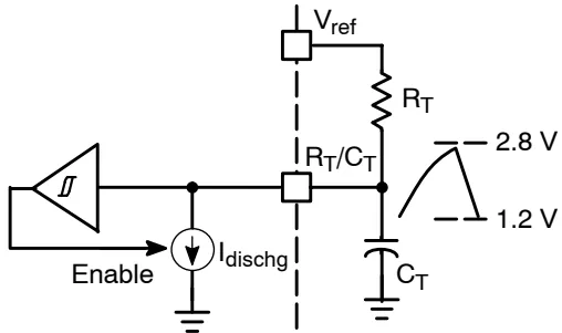
UC3843B datasheet — Figure 18. Oscillator Configuration, p. 8. Reproduced for reference.
The electrical characteristics table provides one specific operating point: switching frequency of 52 kHz typical with R_T = 6.2 kOhm, C_T = 1 nF, and T_j = 25 °C. A separate switching-frequency row lists 500 kHz typical without specifying the accompanying R_T and C_T values.
Figure 3 is titled "Output Dead-Time vs. Oscillator Frequency" on page 5, but the drawing depicts a full test schematic labeled UC2842B rather than a timing curve.
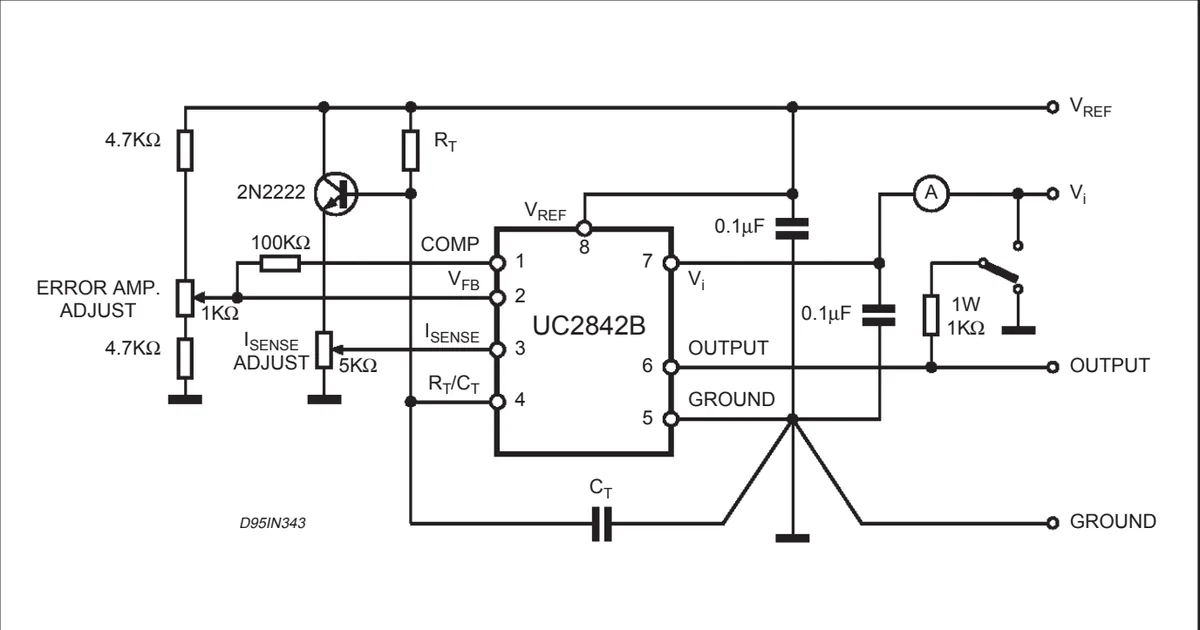
UC3843B datasheet — Figure 3: Output Dead-Time vs. Oscillator Frequency, p. 5. Reproduced for reference.
Current Sensing and Slope Compensation
The untitled current-sense schematic on page 8 depicts the internal current-sense comparator and error amplifier interface using drawing code D95IN347. The current-sense section specifies a propagation delay from the current-sense input to the output of 150 ns typical and 300 ns maximum. Its power supply rejection ratio (PSRR/SVR) is 70 dB typical over V_i = 12 V to 25 V, with no minimum rating stated in that row.
Figure 19 is titled "Isolated MOSFET Drive and Current Transformer Sensing" on page 9, but the schematic illustrates two resistor-based slope compensation configurations tied to the timing network of a UC3842B.
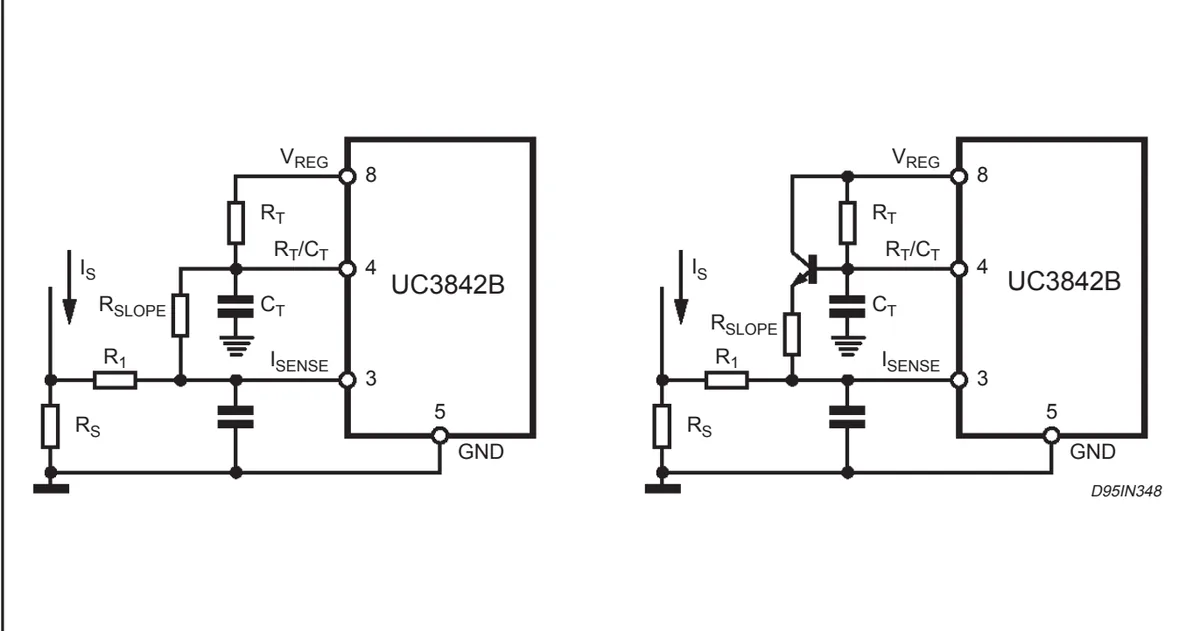
UC3843B datasheet — Figure 19: Isolated MOSFET Drive and Current Transformer Sensing., p. 9. Reproduced for reference.
An untitled schematic on page 9 (drawing D95IN349) presents an isolated power conversion stage with primary current sensing and secondary feedback to calculate peak primary current I_pk.
Error Amplifier and UVLO Thresholds
Figure 16 is titled "Under Voltage Lockout" on page 8, but the drawing contains no UVLO circuit or threshold network; it shows the internal error amplifier connected to external impedances Z_i and Z_f.
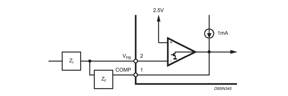
UC3843B datasheet — Figure 16 : Under Voltage Lockout., p. 8. Reproduced for reference.
Because Figure 16 omits UVLO information, thresholds must be referenced from the electrical characteristics tables:
- X843B/5B (including UC3843B): 7.0 V minimum, 7.6 V typical, 8.2 V maximum.
- X842B/4B: 8.5 V minimum, 10.0 V typical, 11.5 V maximum.
Figure 21 details compensation options and pull-down shutdown techniques using discrete bipolar transistors or an SCR tied to pin 1 (COMP).
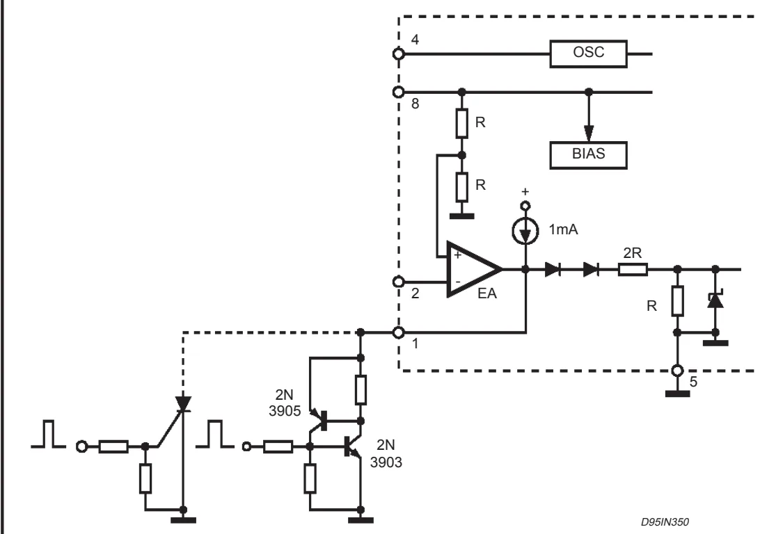
UC3843B datasheet — Figure 21: Error Amplifier Compensation, p. 10. Reproduced for reference.
Page 10 also contains two untitled schematics: one illustrates error amplifier feedback components (R_i, R_d, R_f, C_f) with the 2.5 V reference and 1 mA pull-up source, and the second (drawing D95IN351) shows a current-feedback configuration.
Error amplifier parameters specified in the tables include:
- Unity gain bandwidth: 0.7 MHz minimum, 1 MHz typical at T_J = 25 °C (with a second entry specifying 1 MHz minimum).
- Power supply rejection ratio: 60 dB minimum, 70 dB typical over V_CC = 12 V to 25 V.
- Output sink current: 2 mA minimum, 12 mA typical at V_PIN2 = 2.7 V and V_PIN1 = 1.1 V.
- Inverting input voltage: 2.42 V minimum, 2.5 V typical, 2.58 V maximum at V_PIN1 = 2.5 V.
Synchronization and Duty-Cycle Clamping
Figure 22 illustrates AC-coupling an external clock into the timing node using a 0.01 µF capacitor and a 47 Ohm resistor connected to pin 4(7).
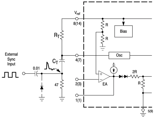
UC3843B datasheet — Figure 22. External Clock Synchronization, p. 12. Reproduced for reference.
Figure 23 demonstrates synchronization and duty-cycle limiting using an external MC1455 timer to drive the oscillator input pin 4(7).
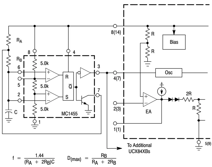
UC3843B datasheet — Figure 23. External Duty Cycle Clamp and Multi-Unit Synchronization, p. 12. Reproduced for reference.
On page 11, an untitled drawing shows a standard NE555 astable oscillator driving a UCX84XA controller, providing formulas for oscillation frequency f and maximum duty cycle D_max. Page 12 includes an untitled block diagram (drawing D95IN355) that outlines external clamp networks for controlling V_CLAMP and peak current I_pk(max).
Current Sensing with SENSEFET and Gate Drive Isolation
Figure 27 demonstrates current sensing using a SENSEFET (specified as MTP10N10M) with a sense resistor R_S = 200 Ohm (1/4 W), yielding the transfer equation V_Pin 5 ≈ 0.075 I_pk.
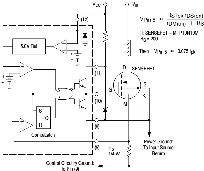
UC3843B datasheet — Figure 27. Current Sensing Power MOSFET, p. 13. Reproduced for reference.
Figure 31 details isolated gate drive and current transformer feedback across an isolation barrier, providing gate drive waveforms at 50% and 25% duty cycle along with the current calculation formula.
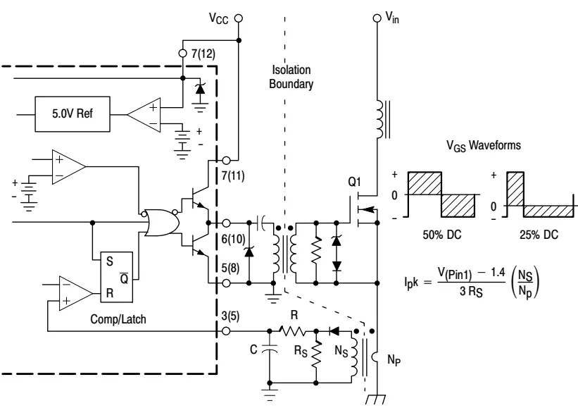
UC3843B datasheet — Figure 31. Isolated MOSFET Drive, p. 14. Reproduced for reference.
Figure 32 illustrates a latched shutdown sub-circuit using either an MCR 101 SCR or discrete 2N3905/2N3903 transistors pulling down pin 1(1).
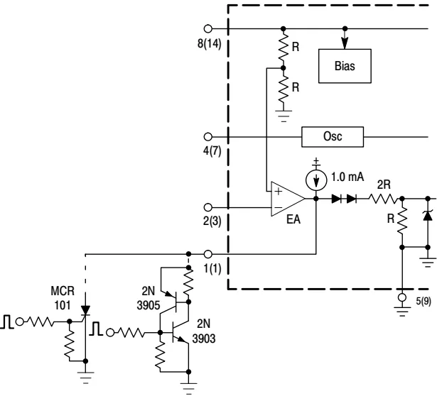
UC3843B datasheet — Figure 32. Latched Shutdown, p. 14. Reproduced for reference.
27 W Off-Line Flyback Reference Circuit
The extracted description labels Figure 35 as an application circuit for the MDA 202; however, the schematic shows the MDA 202 is simply the input bridge rectifier, while the controller is the 8-pin/14-pin PWM IC.
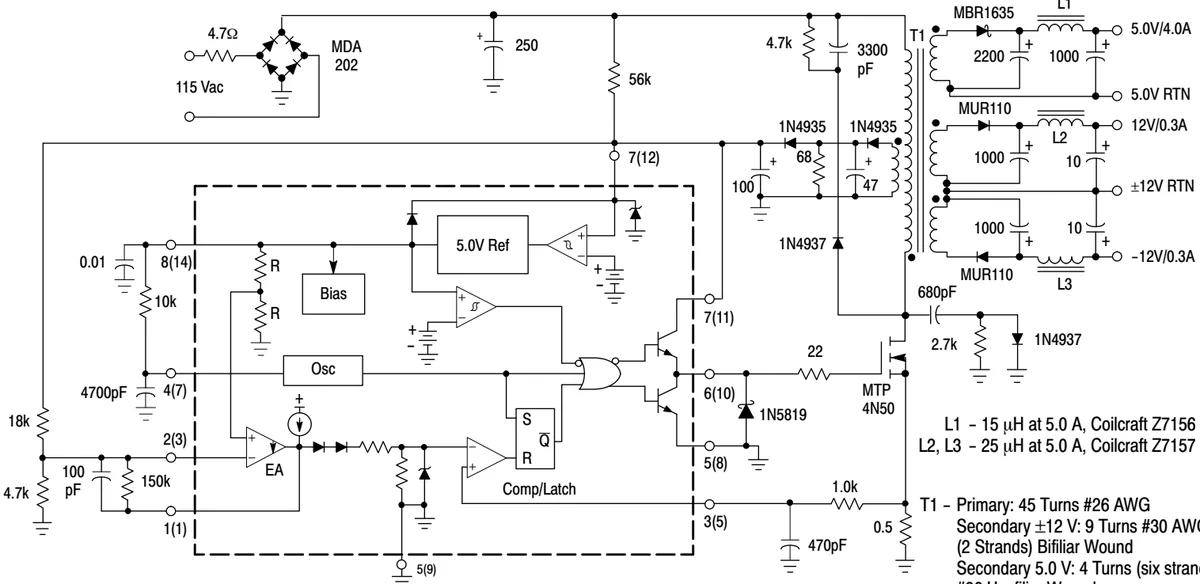
UC3843B datasheet — Figure 35. 27 W Off-Line Flyback Regulator, p. 16. Reproduced for reference.
The specified components in Figure 35 include:
- T1 Transformer: Primary: 45 turns #26 AWG; Secondary ±12 V: 9 turns #30 AWG (2 strands) bifilar wound; Secondary 5.0 V: 4 turns (six strands) #30 AWG.
- Inductors: L1 = 15 µH at 5.0 A (Coilcraft Z7156); L2, L3 = 25 µH at 5.0 A (Coilcraft Z7157).
- Semiconductors: MOSFET MTP 4N50, clamp diode 1N5819, rectifiers MBR1635 and MUR110, diodes 1N4935 and 1N4937.
- Outputs: 5.0 V / 4.0 A, 12 V / 0.3 A, −12 V / 0.3 A.
Known limitation. Figure 35 labels a snubber resistor as 2.7k in series with a 680 pF capacitor, whereas the text inventory transcribed 2.7k as a capacitor and omitted the 680 pF label. The primary current-sense resistor is marked 0.5 Ohm. The datasheet provides no core material, core size, or air gap specifications for transformer T1.
Attribution Discrepancies Across Figures
Several figures in this datasheet cite other part numbers or internal drawing references rather than explicitly naming the UC3843B:
- Figure 3 labels the controller as UC2842B.
- Figure 19 labels the controller as UC3842B.
- Page 8 current-sense schematic is labeled D95IN347.
- Page 9 flyback schematic is labeled D95IN349.
- Figure 21 is labeled D95IN350.
- Page 10 amplifier schematic is labeled D95IN351.
- Page 12 clamp block diagram is labeled D95IN355.
- Figure 23 uses the MC1455 timer as a driver.
- Figure 35 identifies the bridge rectifier as MDA 202.
- Page 11 clock circuit refers generically to UCX84XA.
Known limitation. The datasheet does not publish capacitor dielectric requirements, core geometry or gap sizing for transformer T1, or board layout constraints for high-di/dt loops.
Bring-Up Sequence
- V_CC and UVLO. Verify V_CC reaches the turn-on threshold for the UC3843B (7.0 V minimum, 7.6 V typical, 8.2 V maximum). If supply voltage is limited below 7.0 V, the device will remain in UVLO.
- Startup Current. Verify supply current before turn-on is within 0.312 mA typical and 0.517 mA maximum at V_CC = 6.5 V (or standby current 0.3 mA typical, 0.5 mA maximum).
- Reference Output. Measure pin 8(14) (V_REF). Specified output voltage is 4.9 V minimum, 5.0 V typical, 5.1 V maximum at T_j = 25 °C and I_O = 1 mA.
- Oscillator Operation. With R_T = 6.2 kOhm and C_T = 1 nF at pin 4(7), confirm the ramp oscillates between 1.2 V and 2.8 V at approximately 52 kHz.
- Gate Drive Output. Check pin 6(10) unloaded or with test load. Output rise and fall times are 50 ns typical, 150 ns maximum into C_L = 1.0 nF at 25 °C.
- Current-Sense Limit. Monitor pin 3(5). The propagation delay from pin 3(5) reaching threshold to output turn-off is 150 ns typical, 300 ns maximum.
Troubleshooting
- Controller fails to switch: Check pin 7(12) against the 7.0 V to 8.2 V UVLO threshold window. If the startup supply was sized for the UC3842B/UC3844B (8.5 V to 11.5 V), the UC3843B will start earlier, but if sized below 7.0 V it will never start.
- V_REF is out of range: Measure V_REF at pin 8(14). Note that the datasheet contains two reference rows at T_j = 25 °C and I_O = 1 mA: 4.9 V to 5.1 V in one section, and 4.95 V to 5.05 V in another.
- Switching frequency deviates: Compare the timing components on pin 4(7) with Figure 18. Verify that the ramp waveform swings fully between 1.2 V and 2.8 V.
- Current limit responds slowly: Measure propagation delay from pin 3(5) to pin 6(10) against the 300 ns maximum rating. Verify the RC filter values on pin 3 (in Figure 35, 1.0 kOhm and 470 pF) are not causing excessive phase lag.
- External sync fails: In Figure 22, the sync pulse is AC-coupled via a 0.01 µF capacitor and 47 Ohm resistor directly into pin 4(7). Verify the incoming pulse amplitude is sufficient to overcome the ramp at pin 4(7).
Parametric Inconsistencies
The datasheet includes several typographical anomalies in its electrical tables:
- Reference Voltage: One entry specifies 4.9 V to 5.1 V (T_j = 25 °C, I_O = 1 mA), while another specifies 4.95 V to 5.05 V under the identical test condition.
- Output High State: The row for High State Output Voltage (I_Source = 20 mA) contains an unphysical entry transcribed as 1312.912 V.
- UVLO Minimum Voltage: A table line lists 107.6 V minimum operating voltage in the UVLO section, representing an uncorrected typographic error for 7.6 V.