The STM32G070CB is a 32-bit Cortex-M0+ microcontroller with 128 KB of flash memory, 43 I/O lines, a 12-bit ADC, and a maximum CPU operating frequency of 64 MHz. Its hardware integration requirements are documented across separate sections of the datasheet: clock generation in the oscillator sections, reset filtering in the I/O section, and the analog front-end model in the ADC section.
This article details the specified circuit parameters, conditions, and missing values from the reference figures and parametric tables.
What the Reference Circuit Consists Of
| Sub-circuit | Figure | Page |
|---|---|---|
| Current consumption measurement (VBAT / VDD supply interface) | Section 5.1.7 | 41 |
| 8 MHz crystal oscillator (HSE) | Figure 13 | 55 |
| 32.768 kHz crystal oscillator (LSE) | Figure 14 | 56 |
| NRST pin protection | Figure 17 | 67 |
| ADC input stage and sample-and-hold | untitled figure | 71 |
Section 5.1.7 defines an application setup rather than a formal figure number, but it provides the reference power-supply interface.
Current Consumption Measurement (Section 5.1.7, page 41)
Section 5.1.7 defines the dual-supply test configuration for observing operating current. VBAT connects to the VBAT pin through an I_DDVBAT current source, and VDD (or VDDA) connects to the VDD/VDDA pin through an I_DD current source, with both referenced to ground.
The datasheet specifies no supply decoupling values or target currents in this section. Current consumption figures appear separately in parametric tables under specific operating states. Under "Flash memory enabled; fHCLK = fHSEbypass (<=16 MHz; PLL disabled)" at 16 MHz, typical I_DD is 0.6 mA at 25 °C and 0.7 mA at 85 °C. At 2 MHz with PLL disabled, typical I_DD is 0.219 mA at 25 °C and 0.254 mA at 85 °C. These operating conditions are distinct and must not be combined into an aggregate envelope.
8 MHz Crystal Oscillator (Figure 13, page 55)
Figure 13 illustrates the external high-speed clock interface connected across OSC_IN and OSC_OUT.
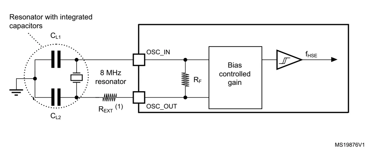
STM32G070CB datasheet — Figure 13. Typical application with an 8 MHz crystal, p. 55. Reproduced for reference.
The caption names an "8 MHz crystal", whereas the drawing labels the component an "8 MHz resonator with integrated capacitors" (C_L1, C_L2). The datasheet does not reconcile whether integrated or discrete load capacitors are intended. The internal feedback resistor R_F and external series resistor R_EXT are unvalued in the schematic.
Application guidance recommends selecting high-quality external ceramic capacitors between 5 pF and 20 pF to match the crystal. The HSE current consumption table is explicitly conditioned on external loads (CL = 5 pF, 10 pF, 20 pF), indicating external capacitors are necessary when using standard discrete crystals:
- 8 MHz (VDD = 3 V, CL = 10 pF): I_DD(HSE) is 0.44 mA typical at Rm = 30 Ohm, and 0.45 mA typical at Rm = 45 Ohm.
- 48 MHz (VDD = 3 V, Rm = 30 Ohm): I_DD(HSE) is 0.68 mA typical at CL = 5 pF, 0.94 mA typical at CL = 10 pF, and 1.77 mA typical at CL = 20 pF.
32.768 kHz Crystal Oscillator (Figure 14, page 56)
Figure 14 provides the low-speed external (LSE) oscillator topology connected across OSC32_IN and OSC32_OUT.
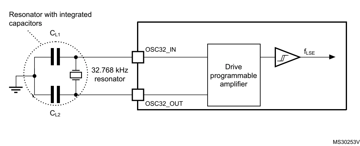
STM32G070CB datasheet — Figure 14. Typical application with a 32.768 kHz crystal, p. 56. Reproduced for reference.
Although the extracted source description attributed this configuration to an "MS30253V IC", the drawing confirms MS30253V1 is ST's internal figure reference code rather than a different device. As with Figure 13, the caption cites a crystal while the drawing depicts a resonator with integrated capacitors (C_L1, C_L2).
The internal drive-programmable amplifier is configured by the LSEDRV[1:0] register bits, which define the drive capability and typical current consumption:
| LSEDRV[1:0] | Drive capability | I_DD(LSE) typical |
|---|---|---|
| 00 | Low | 0.25 uA |
| 01 | Medium low | 0.315 uA |
| 10 | Medium high | 0.5 uA |
| 11 | High | 0.63 uA |
LSE current consumption also varies by supply voltage (VBAT), temperature, and clocking mode:
- Bypass mode (32.768 kHz):
- 2.4 V: 0.286 uA (25 °C), 0.391 uA (85 °C)
- 3.0 V: 0.402 uA (25 °C), 0.523 uA (85 °C)
- 3.6 V: 0.556 uA (25 °C), 0.721 uA (85 °C)
- Crystal mode (32.768 kHz):
- 2.4 V: 0.407 uA (25 °C), 0.528 uA (85 °C)
- 3.0 V: 0.517 uA (25 °C), 0.66 uA (85 °C)
- 3.6 V: 0.66 uA (25 °C), 0.897 uA (85 °C)
Known limitation: Figure 14 provides no capacitance values for C_L1 or C_L2, and the datasheet does not publish required load capacitance specifications or map specific crystals to LSEDRV[1:0] settings.
NRST Pin Protection (Figure 17, page 67)
Figure 17 specifies the hardware interface for external reset generation and filtering.
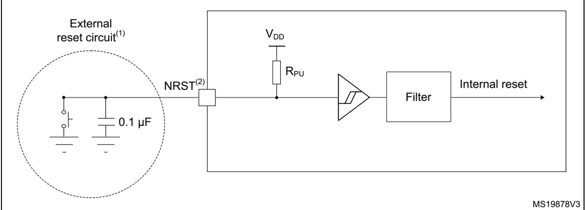
STM32G070CB datasheet — Figure 17. Recommended NRST pin protection, p. 67. Reproduced for reference.
The external reset network consists of an external pushbutton switch and a 0.1 uF capacitor tied to ground. The pull-up resistor R_PU is internal to the microcontroller, connecting the NRST node to V_DD upstream of the Schmitt trigger and internal filter.
Known limitation: The datasheet illustrates the internal pull-up resistor R_PU but omits its numerical resistance value and does not define a required RC time constant for the reset network.
ADC Input Stage (untitled figure, page 71)
The model on page 71 illustrates the analog input network and switched sample-and-hold circuit feeding the 12-bit ADC converter block. It identifies the external source voltage V_AIN, external input resistance R_AIN, pin capacitance C_parasitic, input pin AINx, internal sampling switch resistance R_ADC, sampling capacitor C_ADC, internal test voltage V_T, and leakage current I_Ikg.
This diagram is an equivalent circuit model for calculating sampling time, not a physical bill of materials. The parametric tables leave R_AIN, C_parasitic, R_ADC, and C_ADC unvalued.
ADC sampling is constrained by the ADC operating clock frequency f_ADC:
- Range 1: 140 kHz to 35 MHz
- Range 2: 140 kHz to 16 MHz
These range limits are distinct operating envelopes and must not be merged.
Bringing the Board Up
Follow this sequence to verify the hardware implementation:
- Supply interface (Section 5.1.7, page 41). Confirm regulated voltage arrives at the VDD, VDDA, and VBAT pins relative to ground before releasing the board to run.
- NRST pin (Figure 17, page 67). Verify that the external 0.1 uF capacitor is installed between NRST and GND. Confirm NRST pulls high to V_DD via the internal R_PU.
- HSE clock (Figure 13, page 55). Probe the f_HSE output. If oscillation fails, verify the resonator or crystal network across OSC_IN and OSC_OUT, including the external series damping resistor R_EXT.
- LSE clock (Figure 14, page 56). Probe f_LSE with the 32.768 kHz resonator installed on OSC32_IN and OSC32_OUT. Verify that firmware initializes LSEDRV[1:0] to provide adequate drive strength.
- ADC input (untitled figure, page 71). Confirm analog source signals reach pin AINx, and ensure the ADC clock configuration conforms to Range 1 (140 kHz to 35 MHz) or Range 2 (140 kHz to 16 MHz).
Troubleshooting
- No f_HSE clock output: Inspect the 8 MHz crystal/resonator connections at OSC_IN and OSC_OUT per Figure 13. Because R_EXT is not valued in the datasheet, check the component against the crystal manufacturer's drive-level and damping requirements.
- No f_LSE clock output: Inspect the 32.768 kHz network at OSC32_IN and OSC32_OUT per Figure 14. Increase the drive capability using the LSEDRV[1:0] register bits (00 for Low up to 11 for High) if the oscillator fails to start.
- Device held in reset: Measure the DC level on the NRST pin per Figure 17. Ensure the external 0.1 uF capacitor is not shorted to ground and that the pin reaches V_DD through the internal pull-up resistor R_PU.
- ADC conversion errors: Verify that the source impedance feeding AINx does not violate sampling time constraints derived from the internal model (R_ADC, C_ADC). Confirm f_ADC does not exceed 35 MHz in Range 1 or 16 MHz in Range 2.
- Excessive supply current: Check the measured I_DD against the specific operating state in the parametric tables. Operating at 16 MHz with flash enabled draws 0.6 mA typical at 25 °C (0.7 mA at 85 °C), whereas 2 MHz draws 0.219 mA typical at 25 °C (0.254 mA at 85 °C). Baseline figures change substantially depending on whether the PLL is active and whether the clock source is crystal or bypass.