The SP3485E is a single-channel, single-driver, single-receiver RS-485 transceiver with a 3.3 V nominal supply. Its datasheet carries an extensive set of application and test-circuit figures spanning driver DC and switching test loads, receiver timing, half-duplex bus topologies, and a port protection scheme. Several electrical limits in the parametric tables are conditioned explicitly on these figures (such as "Figure 2, RL=54 Ohm" or "see Fig 3 and Fig 4"), making the test networks an integral part of the electrical specification.
What the Reference Circuit Consists Of
| Sub-circuit | Figure | Page |
|---|---|---|
| Driver DC test load | Fig. 2 Driver DC test load | 9 |
| Driver differential delay and transition time | 图 3 驱动器差分延迟与渡越时间 | 8 |
| Driver propagation delay | 图 4 驱动器传播延迟 | 8 |
| Driver propagation times | Fig. 4 Driver propagation times | 9 |
| Driver test circuit (timing) | 11. Test Circuit | 9 |
| Driver enable/disable times | 图 5 / Fig. 5 Driver enable and disable times | 9 / 10 |
| Driver enable/disable times | 图 6 / Fig. 6 Driver enable and disable times | 9 / 10 |
| Receiver propagation delay test | 图 7 / Fig. 7 Receiver propagation delay | 9 / 10 |
| Receiver enable/disable times | 图 8 接收器使能与禁能时间 | 10 |
| Receiver test configuration (untitled) | (untitled figure) | 11 |
| Bus-type RS-485 half-duplex network | 图 9 / Fig. 9 Bus-type RS485 half-duplex communication network | 11 / 13 |
| Hand-in-hand RS-485 half-duplex network | 图 10 / Fig. 10 Hand-in-hand type RS485 half-duplex communication network | 12 / 13 |
| Port protection scheme | 图 11 / Fig. 11 Port protection scheme | 12 / 14 |
The documentation contains two parallel figure series: a Chinese-numbered series and an English-numbered series. Discrepancies exist between them, so specific figure citations must be tracked individually.
Driver DC Test Load — Fig. 2 (page 9)
Fig. 2 defines the test load against which driver DC output parameters are guaranteed.
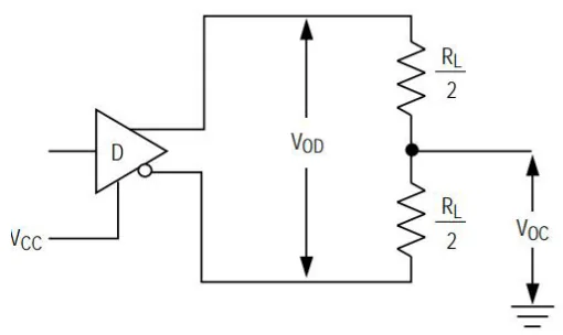
SP3485E datasheet — Fig. 2 Driver DC test load, p. 9. Reproduced for reference.
The parametric tables bind specific limits to this load network:
- Minimum differential output voltage V_OD of 1.5 V under the condition
Figure 2, RL=54 Ohm. - Minimum differential output voltage V_OD of 2.0 V under the condition
Figure 2, RL=100 Ohm. - Maximum change in magnitude of differential output voltage (delta V_OD) of 0.2 V under
Figure 2, RL=54 Ohm. - Maximum change in magnitude of common-mode output voltage (delta V_OC) of 0.2 V under
Figure 2, RL=54 Ohm. - Maximum common-mode output voltage V_OC of 3.0 V under
Figure 2, RL=54 Ohm.
Driver Switching Test Circuits — 图 3 / 图 4 (page 8) and Fig. 4 / Test Circuit (page 9)
Driver switching characteristics are specified across four related figures that carry conflicting load definitions. Fig. 4 shows the arrangement used to define single-ended propagation delays t_PLH and t_PHL.
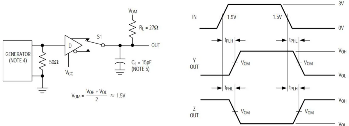
SP3485E datasheet — Fig. 4 Driver propagation times, p. 9. Reproduced for reference.
In Fig. 4 (and 图 4 on page 8), the test conditions define R_L = 27 Ohm, C_L = 15 pF, and V_OM = (V_OH + V_OL)/2 ≈ 1.5 V.
In contrast, 图 3 (page 8) and the "11. Test Circuit" (page 9) define differential timing (t_DD and t_TD) using two capacitors C_L = 15 pF and a differential load resistor R_L = 60 Ohm.
The parametric table under "8. Driver Switching Characteristics" specifies:
- Propagation delay of typ 1 ns, max 8 ns conditioned on
RDIFF = 27 Ohm, (见图 3 与图 4). - Propagation delay of typ 8 ns, max 35 ns conditioned on
RDIFF=27 Ohmand(see Fig 3 and Fig 4).
Known limitation: The datasheet figures conflict on the load resistance, specifying R_L = 60 Ohm in 图 3 and in the "11. Test Circuit" entry, but R_L = 27 Ohm in 图 4 and Fig. 4. The parametric table specifies RDIFF = 27 Ohm while citing both figures simultaneously. The datasheet does not state which figure governs which delay parameter.
Driver Enable and Disable Times — Fig. 5 / Fig. 6 (page 10), 图 5 / 图 6 (page 9)
Driver enable and disable timing is characterised using a 50 pF capacitive load rather than the 15 pF load used for propagation delays. Fig. 5 defines the high-impedance transitions to and from the high output state (t_PZH and t_PHZ).
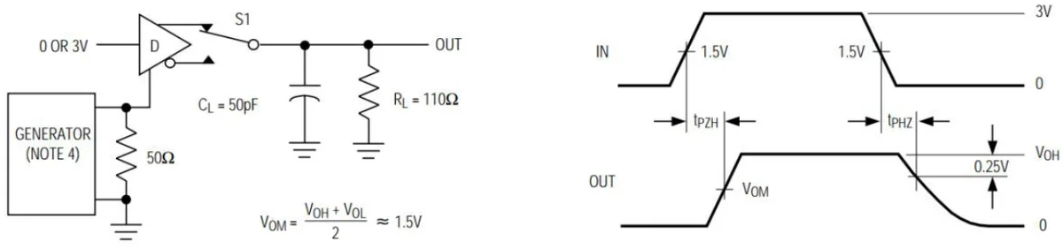
SP3485E datasheet — Fig. 5 Driver enable and disable times, p. 10. Reproduced for reference.
Although the extracted textual description claimed Fig. 5 labeled both intervals as t_PHZ, the schematic in Fig. 5 explicitly labels the turn-on interval as t_PZH and the turn-off interval as t_PHZ, with C_L = 50 pF and R_L = 110 Ohm tied to ground.
Fig. 6 specifies the disable and enable timing for the low output state (t_PSL and t_PLZ) with the 110 Ohm load resistor tied to V_CC.
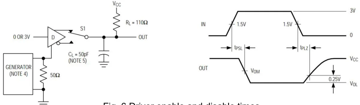
SP3485E datasheet — Fig. 6 Driver enable and disable times, p. 10. Reproduced for reference.
Receiver Propagation Delay — Fig. 7 (page 10), 图 7 (page 9)
Receiver timing parameters t_RPLH and t_RPHL are characterized using the test circuit shown in Fig. 7, configured with C_L = 15 pF and V_OM = V_CC / 2.
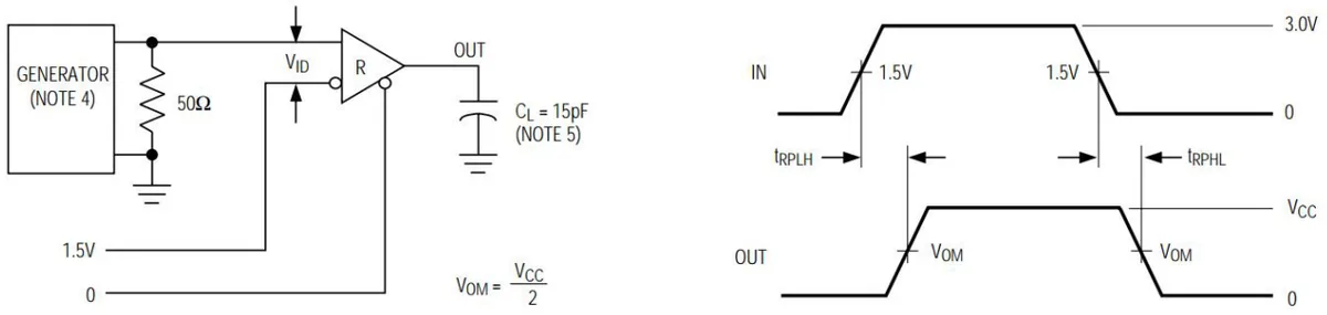
SP3485E datasheet — Fig. 7 Receiver propagation delay, p. 10. Reproduced for reference.
Under "6. Receiver Electrical Characteristics", the datasheet adds two related operating parameters:
- Receiver output low voltage V_OL is max 0.4 V at I_OUT = 2.5 mA and differential input voltage V_ID = −200 mV.
- Data rate is min 10 Mbps (typ 12 Mbps) conditioned on RE = 0 V and DE = 0 V.
Receiver Enable and Disable Times — 图 8 (page 10) and Untitled Figure (page 11)
Receiver output enable and disable timing is described in 图 8 and an untitled figure on page 11. 图 8 defines four switching parameters: t_PRZH, t_PRSH, t_PRZL, and t_PRSL using a 1.5 V / −1.5 V input signal, a 50 Ohm source resistor, and a 1 kOhm pull-up resistor.
Known limitation: The 1 kOhm pull-up resistor in 图 8 is depicted without a stated functional specification, and the untitled page-11 figure lists both a 1 kOhm and a 50 Ohm resistor without identifying the node assignments. The C_L value for 图 8 is omitted entirely.
Bus Topologies — Fig. 9 & Fig. 10 (page 13), 图 9 & 图 10 (pages 11, 12)
The datasheet provides two half-duplex RS-485 network configurations. Fig. 9 illustrates a standard multi-drop bus topology.
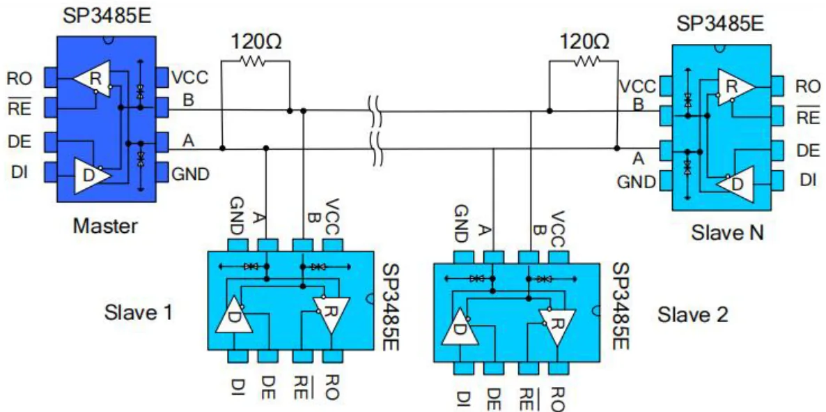
SP3485E datasheet — Fig. 9 Bus-type RS485 half-duplex communication network, p. 13. Reproduced for reference.
Fig. 10 shows an alternate daisy-chained ("hand-in-hand") wiring layout connecting Master and Slave transceivers along lines A and B.
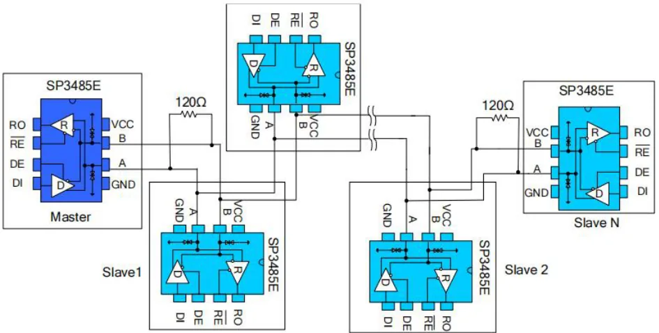
SP3485E datasheet — Fig. 10 Hand-in-hand type RS485 half-duplex communication network, p. 13. Reproduced for reference.
The extracted text descriptions erroneously described 图 9 as an I2C bus with SDA/SCL lines and Fig. 10 as an SPI shift-register network with coupling capacitors; both images actually show RS-485 half-duplex networks using SP3485E transceivers with 120 Ohm termination resistors across lines A and B.
Known limitation: Neither Fig. 9 nor Fig. 10 specifies maximum stub lengths, permissible cable types, maximum node counts, or fail-safe bus biasing networks. Only the two 120 Ohm parallel line terminations are defined.
Port Protection Scheme — Fig. 11 (page 14), 图 11 (page 12)
Fig. 11 provides three interface protection schematics for the bus pins.
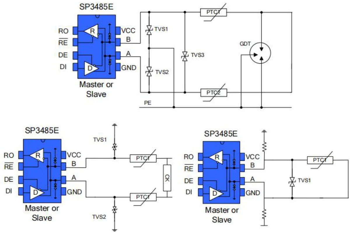
SP3485E datasheet — Fig. 11 Port protection scheme, p. 14. Reproduced for reference.
The top circuit shows three TVS diodes (TVS1 and TVS2 from bus lines B and A to PE; TVS3 across lines A and B), two series PTC fuses (PTC1, PTC2), and a 3-terminal gas discharge tube (GDT) tied between the lines and PE. The lower circuits show simplified configurations with TVS diodes to GND and pull-up/down resistors.
Known limitation: The datasheet names the protection components (TVS1–TVS3, PTC1, PTC2, GDT) but provides no part numbers, standoff voltages, clamping voltages, power ratings, or PTC trip currents.
Operating Limits and Test Conditions
Parametric values in the datasheet are constrained to specific test conditions:
- DC Driver Output Swing: The 1.5 V minimum differential output applies strictly to R_L = 54 Ohm, whereas 2.0 V applies to R_L = 100 Ohm. Unloaded typ output is 3.3 V.
- Supply Current: Current consumption is broken into two distinct states under "7. Supply Current":
- Typical 0.52 mA / maximum 0.8 mA when
/RE = 0 VandDE = 0 V. - Typical 0.54 mA / maximum 0.7 mA when
/RE = VCCandDE = VCC. Do not combine these limits into a single envelope.
- Typical 0.52 mA / maximum 0.8 mA when
- Short-Circuit Limits: Driver output short-circuit current is −250 mA minimum for short circuits to −7 V to 0 V, and +250 mA maximum for short circuits to 0 V to 12 V.
- Operating Temperature: Two discrete temperature grades appear in the specifications: −40 °C to 105 °C and 0 °C to 70 °C. Check the specific orderable suffix to determine the applicable grade.
Bringing the Board Up
- Verify VCC is 3.3 V nominal (3.3 V ± 10%) at the transceiver supply pin with respect to GND.
- Check line terminations against Fig. 9 and Fig. 10: Confirm that 120 Ohm termination resistors are placed across the A and B differential lines at both ends of the bus.
- Verify quiescent current by control pin state:
- In receive mode (
/RE = 0 V,DE = 0 V), verify current is below the 0.8 mA maximum. - In transmit mode (
/RE = VCC,DE = VCC), verify current is below the 0.7 mA maximum.
- In receive mode (
- Measure driver DC differential output across the bus: With a 54 Ohm load resistor across lines A and B per Fig. 2, verify differential swing meets the 1.5 V minimum, common-mode voltage V_OC does not exceed 3.0 V, and delta V_OD and delta V_OC do not exceed 0.2 V.
- Verify receiver output level: With V_ID = −200 mV and I_OUT = 2.5 mA, confirm RO outputs a maximum V_OL of 0.4 V.
Troubleshooting
- Driver output swing below 1.5 V: Measure the differential DC resistance across pins A and B. If equivalent load resistance is lower than 54 Ohm, output voltage is outside the datasheet test condition.
- Driver switching times exceed 35 ns: Check line capacitance and load resistance against Fig. 4. Driver switching limits (1 ns to 8 ns typ, 8 ns to 35 ns max) are specified specifically at RDIFF = 27 Ohm and C_L = 15 pF.
- Enable/disable times do not match specification: Ensure test fixtures use C_L = 50 pF and R_L = 110 Ohm as specified in Fig. 5 and Fig. 6; measurements taken with lighter 15 pF loads will not reflect published values.
- Supply current exceeds 0.7 mA or 0.8 mA: Confirm logic states on DE and /RE. The 0.7 mA limit applies only when both pins are at VCC; the 0.8 mA limit applies only when both are at 0 V.