The PCM5100A is a 2-channel audio DAC with 24-bit resolution, supported sample rates from 8 kHz to 384 kHz, and a maximum clock frequency of 50 MHz. Because format, filter, de-emphasis, and mute are configured by hardware pin strapping rather than an internal register bus, the external pin networks form the entire configuration interface.
| Sub-circuit | Figure | Page |
|---|---|---|
| System-level integration (PCM1863/5 + PCM510xA + MSP430) | 4, Simplified System Diagram | 1 |
| Hardware-controlled subsystem: audio interface, supplies, output stages | 33, Simplified Schematic, Hardware-Controlled Subsystem | 26 |
| XSMT mute control from MCU GPIO | 38, Using the XSMT Pin | 30 |
| XSMT in external UVP mode | 39, XSMT in External UVP Mode | 31 |
| Package pinout, power and ground routing | 43, PCM510x Layout Example | 34 |
Figure 4 — System-Level Integration
Figure 4 is a block diagram illustrating system-level interconnections between a PCM1863/5 ADC, a PCM510xA DAC, and an MSP430 host microcontroller across I²S, BCK, and LRCK lines. It scopes the architecture to the broader PCM510xA family rather than providing a component-level netlist or passive values specific to the PCM5100A.
Figure 33 — Hardware-Controlled Subsystem
Figure 33 provides the primary reference schematic for the hardware-controlled configuration.
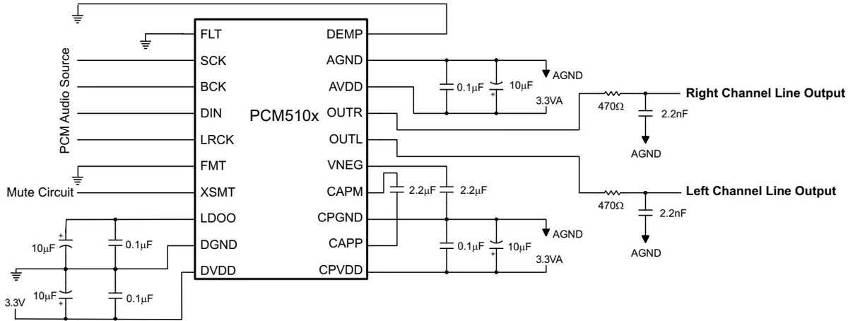
PCM5100A datasheet — Figure 33. Simplified Schematic, Hardware-Controlled Subsystem, p. 26. Reproduced for reference.
The drawing specifies the following operating limits and component requirements:
- Control strapping: Control pins FLT, DEMP, and FMT configure the digital filter, de-emphasis, and audio format directly without software registers.
- Supply rail limits: Dual 3.3 V rails power the device. Recommended operating conditions specify 3.1 V min / 3.3 V typ / 3.46 V max for 3.3 V DVDD and CPVDD (referenced to CPGND). The separate power supply requirements table specifies a wider range of 3.0 V min / 3.3 V typ / 3.6 V max for DVDD, AVDD, and CPVDD. Keep these distinct parametric scopes separate.
- Decoupling and charge pump: Decoupling on DVDD, AVDD, CPVDD, and LDOO requires parallel 0.1 µF and 10 µF capacitors. Flying capacitors for charge pump pins CAPP/CAPM and VNEG require 2.2 µF.
- Line output stages: Analog outputs OUTL and OUTR are scoped for a typical output voltage of 2.1 V and a typical load capacitance of 10 pF (clout). Each output feeds a series 470 Ω resistor and a 2.2 nF shunt capacitor to AGND.
Known limitation: Figure 33 specifies capacitance values (0.1 µF, 2.2 µF, 10 µF) and resistance values (470 Ω) but omits dielectric types, voltage ratings, package sizes, and component tolerances.
Figure 38 — XSMT Mute Control
Figure 38 details hardware mute control driven from a host MCU GPIO.
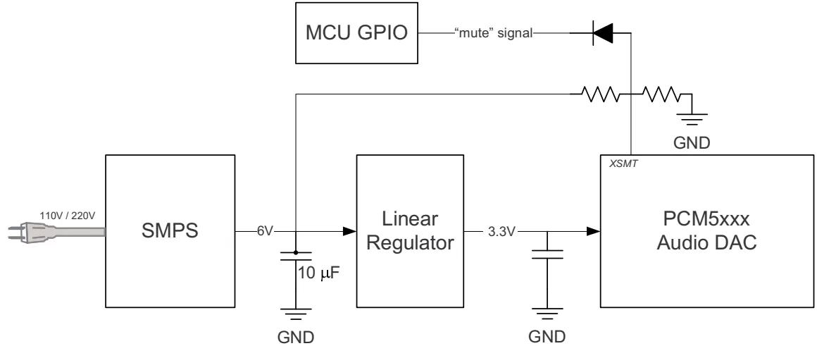
PCM5100A datasheet — Figure 38. Using the XSMT Pin, p. 30. Reproduced for reference.
A 6 V pre-regulator rail feeds a linear regulator supplying 3.3 V to the DAC, while a resistor divider off the 6 V rail biases the XSMT pin. An MCU GPIO controls XSMT through a steering diode (cathode to GPIO).
Regardless of the drive topology, the timing requirements section for XSMT mandates that the rise time (tr) and fall time (tf) on the XSMT pin must each not exceed 20 ns.
Known limitation: Figure 38 omits resistance values for the divider, the linear regulator output capacitor value, and the part number or specifications for the steering diode.
Figure 39 — XSMT in External UVP Mode
Figure 39 provides an alternate network for the XSMT pin configured for external under-voltage protection (UVP).
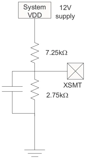
PCM5100A datasheet — Figure 39. XSMT in External UVP Mode, p. 31. Reproduced for reference.
The circuit divides a 12 V System VDD rail using a 7.25 kΩ high-side resistor and a 2.75 kΩ low-side resistor, with a filter capacitor in parallel with the 2.75 kΩ resistor.
Known limitation: Figure 39 omits the capacitance value for the parallel filter capacitor and gives no tolerance ratings for the 7.25 kΩ and 2.75 kΩ resistors. The documentation does not define arbitration or switching circuitry to combine this UVP circuit with the active GPIO mute circuit from Figure 38.
Figure 43 — Layout Example
Figure 43 illustrates component placement, routing, and copper pours on a 20-pin package.
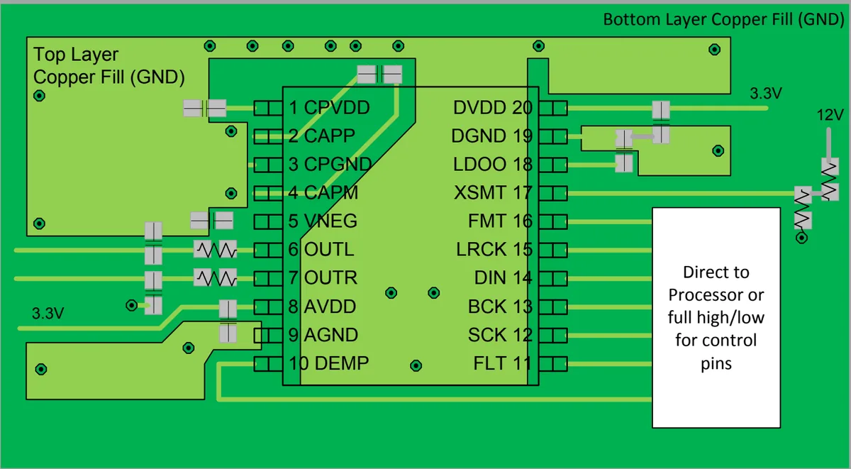
PCM5100A datasheet — Figure 43. PCM510x Layout Example, p. 34. Reproduced for reference.
Notable floorplan details include:
- Pin assignment partitioning: The left side carries charge pump and analog pins (CPVDD, CAPP, CPGND, CAPM, VNEG, OUTL, OUTR, AVDD, AGND, DEMP). The right side carries digital supplies, clock, data, and control routing (DVDD, DGND, LDOO, XSMT, FMT, LRCK, DIN, BCK, SCK, FLT). DEMP (pin 10) routes across the board beneath the IC to join the digital control cluster.
- XSMT implementation: The layout implements the external UVP divider from Figure 39, wiring pin 17 through two resistors to a 12 V rail and ground. The 12 V rail supplies only this UVP divider network; all DAC supply pins remain at 3.3 V.
Known limitation: Figure 43 does not specify layer stackup, PCB trace widths, copper weights, or via drill geometries.
The Non-Obvious Constraint: Two Different XSMT Networks
Figures 38 and 39 describe mutually exclusive drive networks for pin 17 (XSMT):
- Figure 38 provides active microcontroller mute control via a diode pull-down and a divider off the 6 V pre-regulator rail.
- Figure 39 (and the layout in Figure 43) implements external UVP monitoring using a dedicated 7.25 kΩ / 2.75 kΩ divider tied to a 12 V system supply.
The datasheet provides no hybrid schematic incorporating both functions simultaneously. Selecting external UVP per Figure 39 or active MCU mute per Figure 38 must be resolved before board layout, keeping the 20 ns maximum tr and tf switching constraint intact.
Bringing the Board Up
- Verify power rails against Figure 33: Ensure AVDD, DVDD, and CPVDD are within 3.1 V to 3.46 V under recommended operating conditions (absolute maximum is 3.9 V).
- Check charge-pump and LDO pins: Confirm 2.2 µF capacitors are populated across CAPP and CAPM, and from VNEG to CPGND. Verify 0.1 µF and 10 µF capacitors are populated on LDOO and DVDD.
- Verify XSMT circuit selection: Check whether pin 17 is populated with the Figure 38 GPIO network or the Figure 39 7.25 kΩ / 2.75 kΩ divider. Confirm that 12 V is tied only to the UVP divider, never directly to DAC power pins.
- Inspect strapping pins: Confirm FLT, DEMP, and FMT pins are tied to ground or logic rails according to the intended audio format and filter mode.
- Verify input clocks: Ensure SCK, BCK, and LRCK frequencies do not exceed the 50 MHz maximum system clock limit across supported sample rates (8 kHz to 384 kHz).
- Measure analog outputs: Verify line outputs at OUTL and OUTR swing around typical 2.1 V levels into the 470 Ω and 2.2 nF reconstruction filter.
Troubleshooting
- No audio output on either channel: Inspect the voltage at XSMT (pin 17). If held low by the Figure 38 GPIO diode circuit or held below threshold by the Figure 39 UVP divider, the DAC outputs remain muted.
- Audio present on one channel only: Check component population on the silent channel's output filter (470 Ω series resistor and 2.2 nF shunt capacitor to AGND) against Figure 33.
- Incorrect audio framing or pitch: Check the FMT pin strapping state against Figure 33 and confirm the input sample rate is within the 8 kHz to 384 kHz range.
- Charge pump failure / excessive rail ripple: Verify flying capacitors on CAPP/CAPM (2.2 µF) and decoupling capacitors on CPVDD and VNEG (10 µF / 0.1 µF and 2.2 µF) are securely soldered and not shorted to ground.
- Excessive XSMT switching transients: Measure rise and fall times on pin 17 with an oscilloscope. Ensure tr and tf do not exceed the 20 ns datasheet maximum.