The LAN8720A is a 10/100 Ethernet PHY in a 24-QFN package that interfaces to a MAC over RMII and to the cable through external magnetics and an RJ45 jack. While the external component count is low, nearly every part is critical, and two LED pins double as hardware configuration straps latched at reset.
The datasheet defines the application circuit across several dedicated diagrams rather than a single schematic:
| Sub-circuit | Figure / Section | Page |
|---|---|---|
| Power supply, internal regulator enabled | FIGURE 3-16 | 37 |
| Power supply, 1.2 V external source | FIGURE 3-17 | 38 |
| Twisted-pair interface, single supply | FIGURE 3-18 | 39 |
| Twisted-pair interface, dual supplies | FIGURE 3-19 | 40 |
| LED / configuration strap polarity | FIGURE 3-10, FIGURE 3-11 | 32 |
| Crystal network (300 µW and 100 µW variants) | §63–64 | 63, 64 |
| Legacy copper interface | FIGURE 7-5 | 72 |
Power: Two Topologies
The LAN8720A requires a 3.3 V analog rail and a 1.2 V core rail (VDDCR). The core rail can be generated internally or supplied externally, chosen by the REGOFF strap pin at reset:
Internal regulator enabled (FIGURE 3-16, p. 37). A 3.3 V rail supplies VDD1A and VDD2A. VDD2A powers the internal regulator input, which outputs 1.2 V on VDDCR.
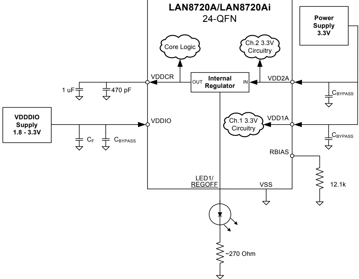
LAN8720A datasheet — FIGURE 3-16: POWER SUPPLY DIAGRAM (1.2V SUPPLIED BY INTERNAL REGULATOR), p. 37. Reproduced for reference.
External 1.2 V source (FIGURE 3-17, p. 38). The internal regulator is disabled via strapping, and an external 1.2 V supply connects directly to VDDCR.
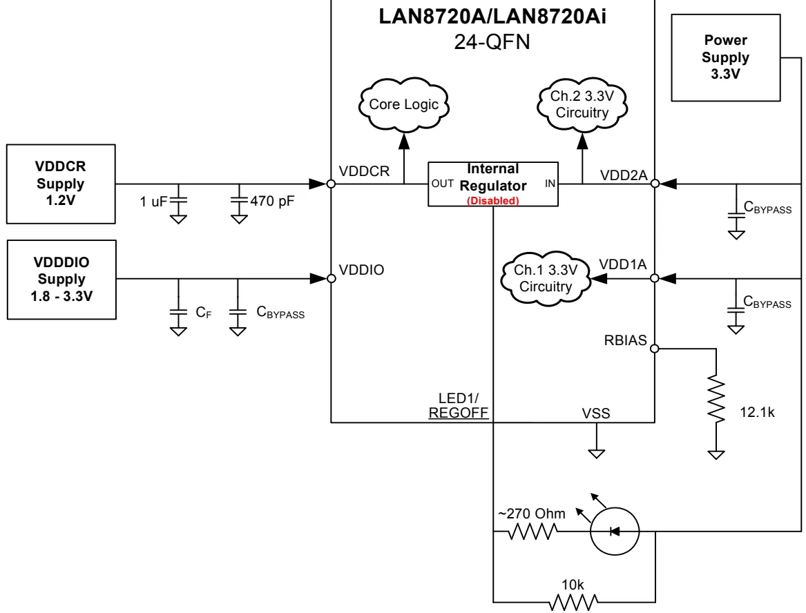
LAN8720A datasheet — FIGURE 3-17: POWER SUPPLY DIAGRAM (1.2V SUPPLIED BY EXTERNAL SOURCE), p. 38. Reproduced for reference.
Resistor and Rail Discrepancies
- RBIAS pull-down: FIGURE 3-16 and FIGURE 3-17 specify 12.1 kΩ (1% standard E96 value) to set the internal analog bias current. In contrast, FIGURE 7-5 on page 72 specifies 12 kΩ and explicitly labels the device as the older LAN8720 rather than the LAN8720A. Use 12.1 kΩ for the LAN8720A.
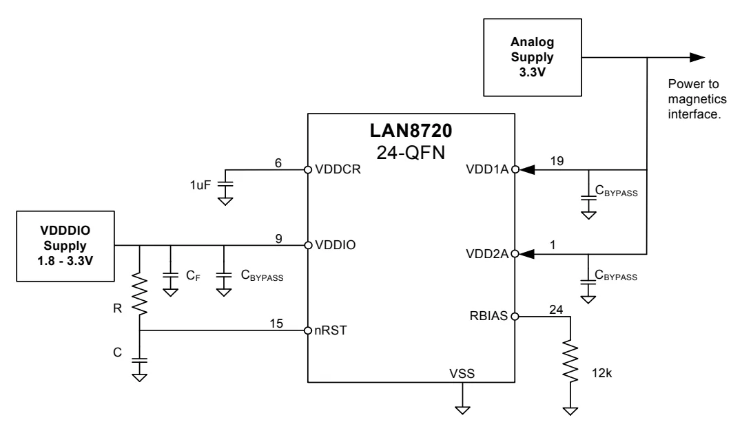
LAN8720A datasheet — FIGURE 7-5: COPPER INTERFACE DIAGRAM, p. 72. Reproduced for reference.
- VDDIO operating range: Application figures mark VDDIO as 1.8–3.3 V, whereas the electrical characteristics table specifies an absolute operating supply voltage range of 1.62–3.6 V. Design nominal rails to sit within 1.8–3.3 V.
Known limitation: The datasheet specifies bypass capacitors (
1 µF,470 pF,C_BYPASS,C_F), but does not publish capacitor dielectric types, ESR, tolerances, voltage ratings, or specific layout distance constraints.
The Twisted-Pair Interface
The MDI interface requires four 49.9 Ω termination resistors, a magnetics module, 75 Ω terminations on the RJ45 side, and a high-voltage decoupling capacitor.
Single supply (FIGURE 3-18, p. 39). A single 3.3 V supply powers VDD1A, VDD2A, and the magnetics center taps through a ferrite bead.
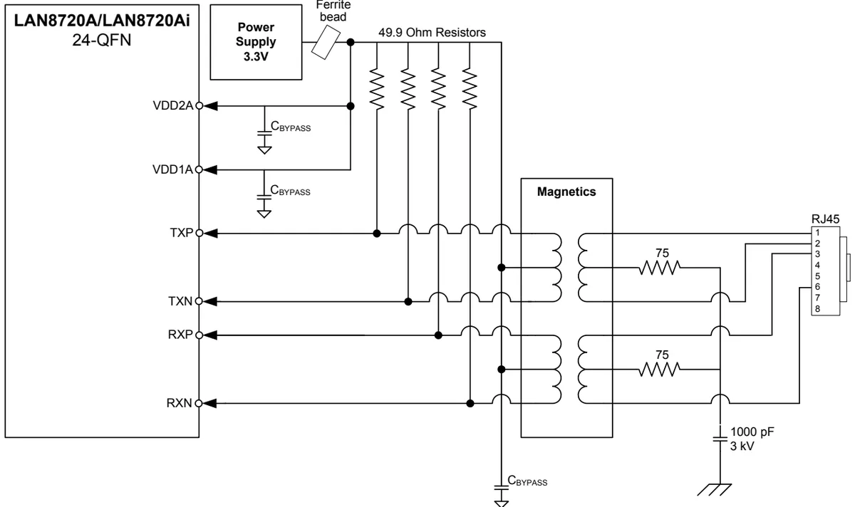
LAN8720A datasheet — FIGURE 3-18: TWISTED-PAIR INTERFACE DIAGRAM (SINGLE POWER SUPPLY), p. 39. Reproduced for reference.
The extracted text description for FIGURE 3-18 refers to a "Gigabit Ethernet PHY interface," but the LAN8720A is strictly a 10/100 Ethernet transceiver supporting 10BASE-T and 100BASE-TX.
Dual supplies (FIGURE 3-19, p. 40). The PHY analog rails remain at 3.3 V, while the magnetics center taps are powered from an independent 2.5–3.3 V supply without a ferrite bead.
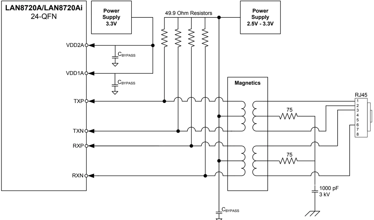
LAN8720A datasheet — FIGURE 3-19: TWISTED-PAIR INTERFACE DIAGRAM (DUAL POWER SUPPLIES), p. 40. Reproduced for reference.
Key MDI implementation details:
- Termination resistors: 49.9 Ω, 1%, on TXP, TXN, RXP, and RXN.
- Cable isolation capacitor: 1000 pF, 3 kV from the 75 Ω common-mode node to chassis ground. Substituting a lower-voltage part is not equivalent; the figures specify the 3 kV rating.
Known limitation: The datasheet does not specify magnetics part numbers, turns ratio, inductance, or recommended integrated RJ45 jacks.
Clocking: 50 MHz Clock In vs. 25 MHz Crystal
The LAN8720A supports two clocking modes:
- External 50 MHz reference clock (FIGURE 3-7, p. 29): Supplied to XTAL1/CLKIN. The nINT interrupt function is supported in this mode.
- 25 MHz fundamental crystal (FIGURE 3-8, p. 30): Connected across XTAL1 and XTAL2. The PHY outputs a 50 MHz RMII reference clock on REFCLKO. In this mode, nINT is disabled because the pin is repurposed for REFCLKO.
The crystal interface is documented in two drive variants:
| Variant | Components | Source |
|---|---|---|
| 300 µW crystal | Crystal Y1 across XTAL1/XTAL2, load capacitors C1 and C2 to ground | p. 63 |
| 100 µW crystal | Crystal Y1, series resistor Rs between XTAL2 and crystal, C1 and C2 to ground | p. 64 |
Crystal specifications mandate a load capacitance of 8–12 pF and operating temperature up to 85 °C.
Known limitation: The datasheet does not supply explicit values for C1, C2, or Rs. C1 and C2 depend on stray PCB capacitance and crystal load specs; Rs must be calculated to prevent overdriving 100 µW crystals.
Configuration Straps: LED Pins Latch at Reset
The LED1 and LED2 pins are multi-function: they serve as status outputs during normal operation, but their voltage levels are sampled on the rising edge of nRST to latch operating modes.
- LED1/REGOFF: Selects regulator mode. Pulling low (REGOFF = 0) enables the internal 1.2 V regulator; pulling high (REGOFF = 1) disables it.
- LED2/nINTSEL: Selects interrupt mode polarity and pin function.
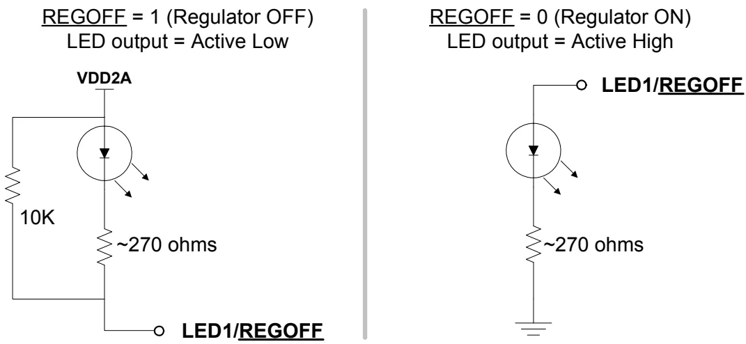
LAN8720A datasheet — FIGURE 3-10: LED1/REGOFF POLARITY CONFIGURATION, p. 32. Reproduced for reference.
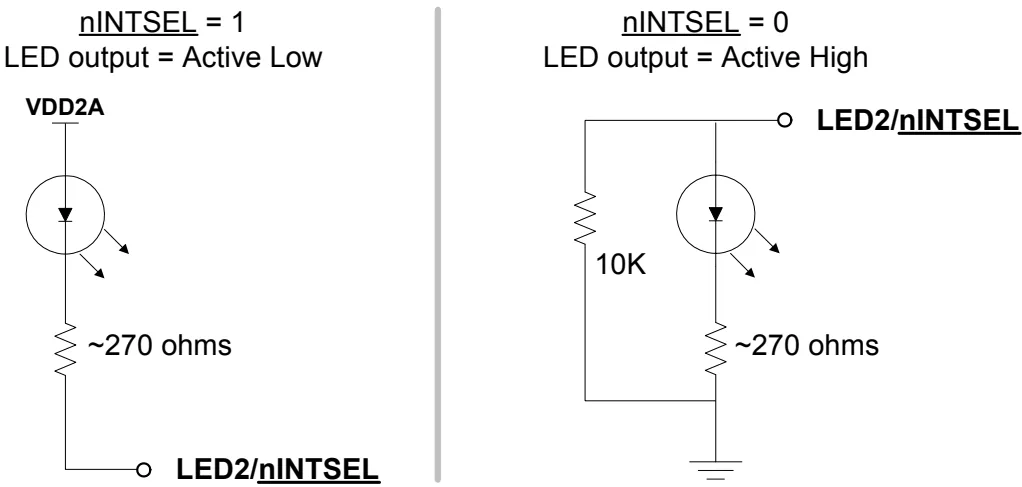
LAN8720A datasheet — FIGURE 3-11: LED2/NINTSEL POLARITY CONFIGURATION, p. 32. Reproduced for reference.
| Pin | Strap Value | LED Active State | Circuit Implementation |
|---|---|---|---|
| LED1/REGOFF | REGOFF = 1 (Regulator OFF) | Active Low | 10 kΩ pull-up to VDD2A, ~270 Ω series resistor to LED |
| LED1/REGOFF | REGOFF = 0 (Regulator ON) | Active High | ~270 Ω series resistor and LED to ground, no pull-up |
| LED2/nINTSEL | nINTSEL = 1 | Active Low | LED and ~270 Ω series resistor to VDD2A |
| LED2/nINTSEL | nINTSEL = 0 | Active High | 10 kΩ pull-up to VDD, LED and ~270 Ω resistor to ground |
If an LED is placed without matching the strap pull-up or pull-down requirements, the regulator state will configure incorrectly at power-on. Configuration strap timing requires meeting setup time t_css and hold time t_csh around reset relative to the 80% supply threshold (FIGURE 5-3, p. 59).
Bring-Up and Troubleshooting Checklist
- Verify Power Rails: Check VDDIO (1.8–3.3 V nominal) and ensure VDDCR stabilizes at 1.2 V. If using the internal regulator, ensure VDD2A reaches 3.3 V.
- Read Configuration Straps: Query the PHY control registers over SMI/MDIO to confirm REGOFF and nINTSEL latched as intended.
- Verify RBIAS: Measure the resistance on pin 24 to ground; confirm it is fitted with 12.1 kΩ (not open, grounded, or 12 kΩ).
- Inspect Clocks: For a 25 MHz crystal, check for a 50 MHz output on REFCLKO. For an external 50 MHz oscillator, verify clock amplitude and frequency at XTAL1/CLKIN.
- Connector Loopback: §3.8.8.3 defines an RJ45 loopback test connecting pin 1 to pin 3 and pin 2 to pin 6. This validates the MAC, PHY, and magnetics path independently of cable runs.
- Output Signal Levels: Transmit amplitude must meet 0.95–1.05 V peak-to-peak for 100BASE-TX, or 2.2–2.8 V (2.5 V typical) for 10BASE-T. Out-of-spec amplitudes indicate incorrect termination (check the 49.9 Ω resistors) or incorrect center-tap voltage.