The ADS1220 is a precision 24-bit delta-sigma ADC with an integrated PGA and reference, taking two differential or four single-ended inputs through an input multiplexer, at up to 2 kSPS. It is aimed at measuring small sensor signals, and its datasheet documents three primary sensor measurement topologies — thermocouple, 3-wire RTD, and resistive bridge — alongside dedicated figures for the serial interface, supply configurations, and PCB layout. Each circuit specifies distinct external passive networks and pin assignments. This guide reviews the published topologies, notes the exact values provided, and highlights where specifications or figure descriptions conflict.
Reference Circuit Summary
| Sub-circuit | Figure | Page |
|---|---|---|
| K-Type thermocouple measurement (overview) | — | 1 |
| Analog input multiplexer (internal) | Figure 8-1 | 20 |
| Simplified PGA diagram (internal) | Figure 8-2 | 21 |
| Example where V_CM is at lowest limit | Figure 8-6 | 24 |
| Serial interface connections | Figure 9-1 | 47 |
| Thermocouple measurement | Figure 9-3 | 52 |
| 3-wire RTD measurement | Figure 9-6 | 55 |
| Resistive bridge measurement | Figure 9-11 | 62 |
| Unipolar analog power supply | Figure 9-13 | 64 |
| Bipolar analog power supply | Figure 9-14 | 64 |
| System component placement | Figure 9-15 | 65 |
| Layout example | Figure 9-16 | 66 |
Internal Architecture Figures
Figure 8-1 (page 20) details the internal analog front end. The analog input pins feature multiplexed roles: AIN0 shares a physical pin with positive reference REFP1, and AIN3 shares a pin with negative reference REFN1. The routing includes two matched excitation current sources (IDAC1, IDAC2), a 10 µA burnout current source switchable to either PGA input, internal system monitors, and a low-side power switch connecting AIN3/REFN1 to AVSS.
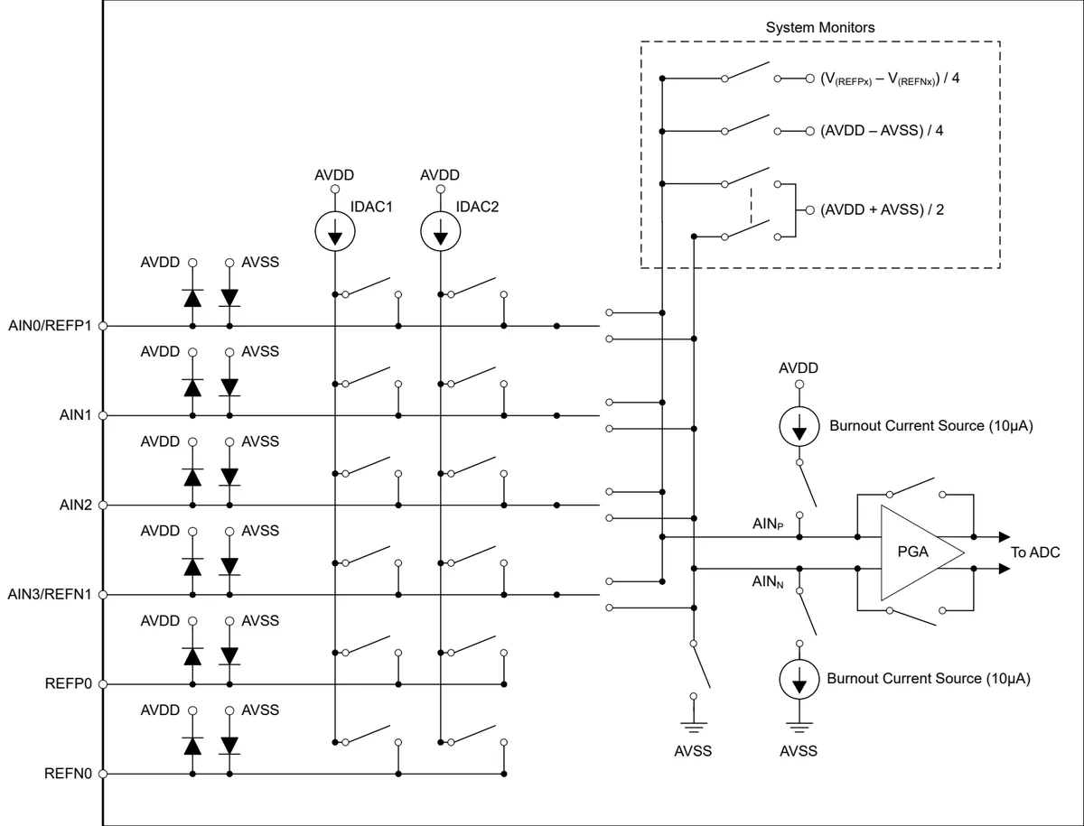
ADS1220 datasheet — Figure 8-1. Analog Input Multiplexer, p. 20. Reproduced for reference.
Figure 8-2 (page 21) shows the differential programmable gain amplifier stage. The internal differential inputs AIN_P and AIN_N pass through internal 200 Ohm series resistors and 25 pF filter capacitors to ground before entering the op-amp buffers, giving an overall transfer function of V_OUT = Gain × V_IN.
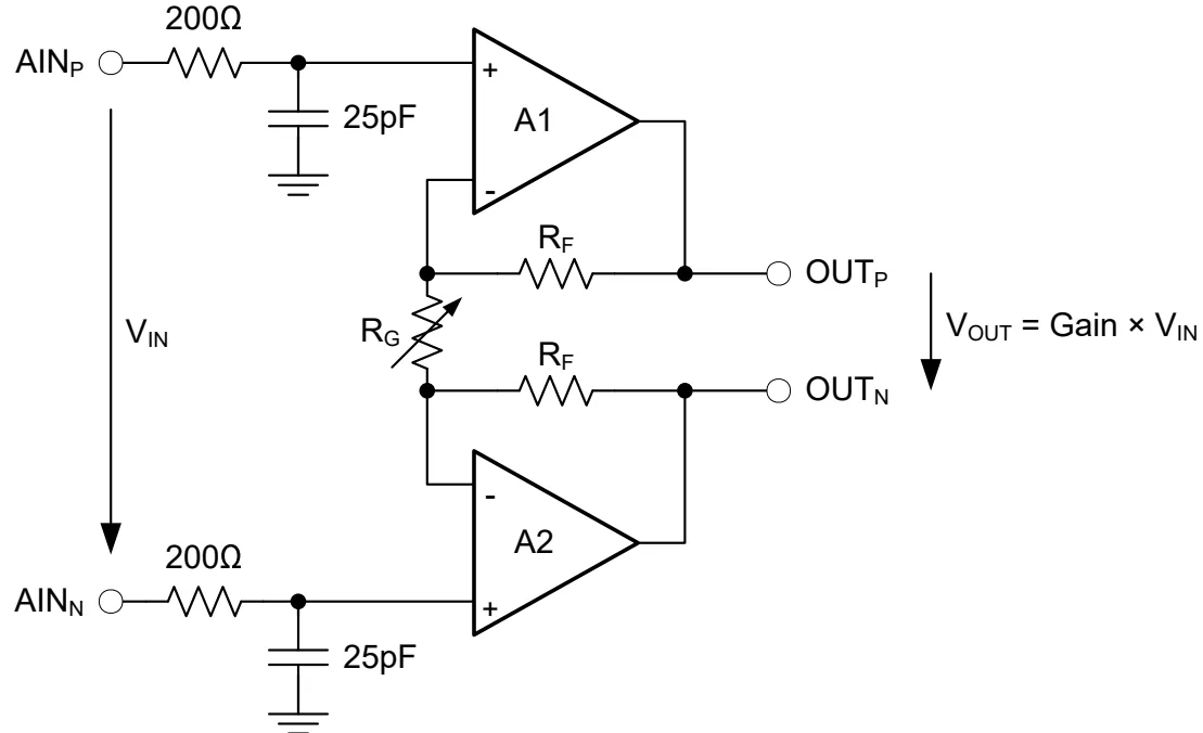
ADS1220 datasheet — Figure 8-2. Simplified PGA Diagram, p. 21. Reproduced for reference.
Figure 8-6 (page 24) illustrates the internal PGA operation when input common-mode voltage V_CM is at its lowest limit. The example operates at V_CM = 1.0 V with input voltages V(AINP) = 1.05 V and V(AINN) = 0.95 V (50 mV per side, 100 mV differential). With the gain-setting resistor set to R_F / 7.5 (Gain = 16), the outputs swing 800 mV per side around common mode to V(OUTP) = 1.8 V and V(OUTN) = 0.2 V, producing a 1.6 V differential output.
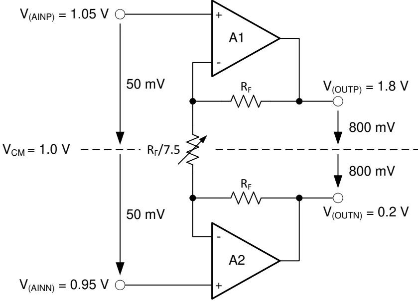
ADS1220 datasheet — Figure 8-6. Example Where V_CM is at Lowest Limit, p. 24. Reproduced for reference.
Serial Interface
Figure 9-1 (page 47) connects a host microcontroller SPI interface to the ADS1220. The digital lines (SCLK, CS, DIN, DOUT/DRDY, and DRDY) each incorporate a 47 Ohm series resistor. Decoupling capacitors of 0.1 µF are placed on DVDD and AVDD at 3.3 V, while CLK (pin 3) is tied directly to DGND. While the extracted datasheet text description mistakenly stated pin 11 was REFP1 without AIN0, the drawing clearly labels pin 11 as AIN0/REFP1. Both DOUT/DRDY (pin 15) and a standalone DRDY line (pin 14) are brought out.
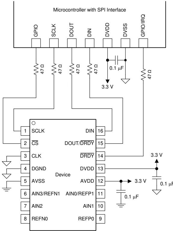
ADS1220 datasheet — Figure 9-1. Serial Interface Connections, p. 47. Reproduced for reference.
Thermocouple Measurement
Figure 9-3 (page 52) shows the thermocouple measurement configuration using AIN0 and AIN1, operating from 3.3 V supplies with 0.1 µF decoupling on AVDD and DVDD. Biasing resistors R_B1 and R_B2 set the DC operating point on the inputs. The external anti-aliasing filter consists of resistors R_F1 and R_F2 and capacitors C_CM1, C_CM2, and C_DIF.
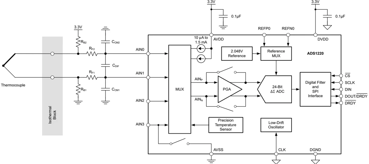
ADS1220 datasheet — Figure 9-3. Thermocouple Measurement, p. 52. Reproduced for reference.
Known limitation: The datasheet text specifies R_F1 = R_F2 = 1 kOhm, C_DIF = 100 nF, and C_CM1 = C_CM2 = 10 nF. Do not confuse these external filter values with the internal 200 Ohm / 25 pF network shown inside the PGA in Figure 8-2.
3-Wire RTD Measurement
Figure 9-6 (page 55) shows the ratiometric 3-wire RTD configuration. The internal current sources IDAC1 and IDAC2 output through AIN2 and AIN3 to cancel lead resistances R_LEAD1, R_LEAD2, and R_LEAD3. Return current (I_IDAC1 + I_IDAC2) passes through reference resistor R_REF to ground, generating the differential reference between REFP0 and REFN0.
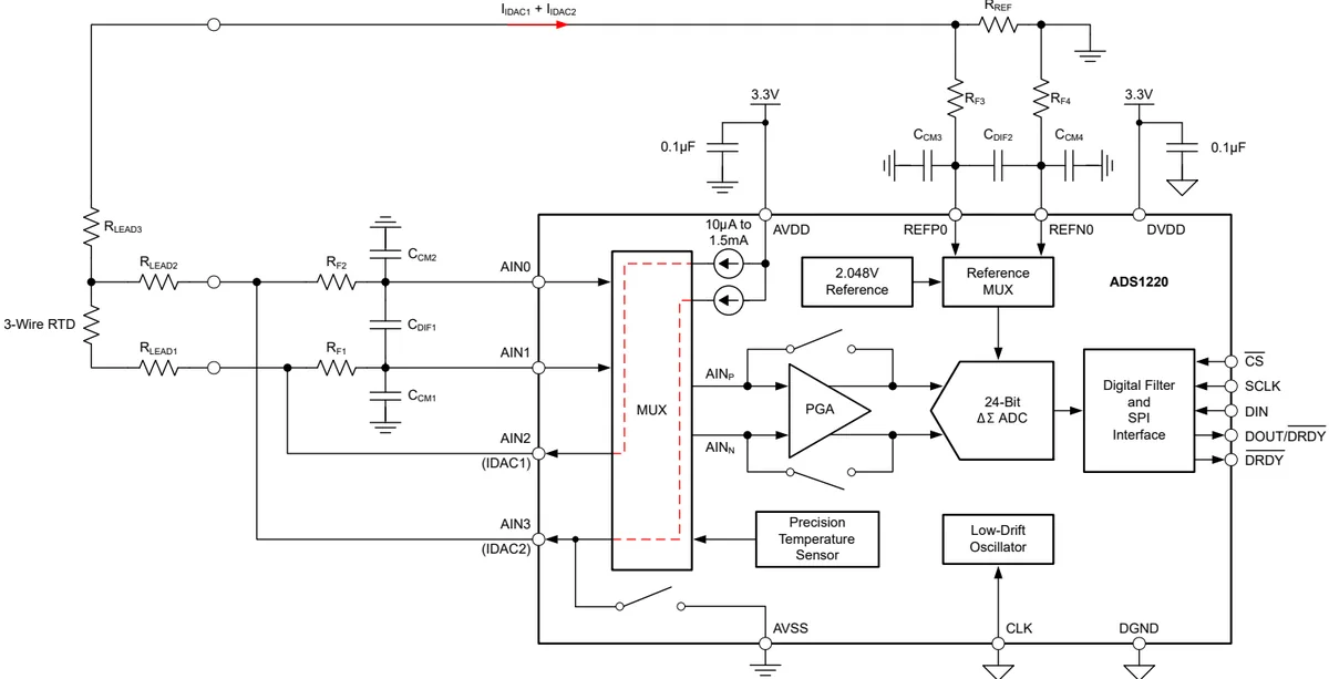
ADS1220 datasheet — Figure 9-6. 3-Wire RTD Measurement, p. 55. Reproduced for reference.
Known limitation: The datasheet calculates R_REF = V_REF / (I_IDAC1 + I_IDAC2) = 1.65 V / 1 mA = 1.65 kOhm. The reference inputs require a matched filter (R_F3, R_F4, C_DIF2, C_CM3, C_CM4) whose cutoff frequency matches the input filter (R_F1, R_F2, C_DIF1, C_CM1, C_CM2). Lead resistances R_LEAD1–R_LEAD3 depend on cabling and are unvalued.
Resistive Bridge Measurement
Figure 9-11 (page 62) implements a ratiometric bridge measurement using a 5.0 V excitation source. Here AVDD is powered at 5.0 V with a 0.1 µF capacitor, while DVDD remains at 3.3 V with a 0.1 µF capacitor. The bridge excitation lines connect to reference inputs REFP1 and REFN1, with differential capacitor C_DIF2 placed directly across them. The bridge differential signal routes through R_F1, R_F2, C_CM1, C_CM2, and C_DIF1 to AIN1 and AIN2. The low-side switch connects REFN1 to AVSS to enable sensor power cycling. Note that contrary to its text description, the figure drawing includes both DOUT/DRDY and dedicated DRDY lines.
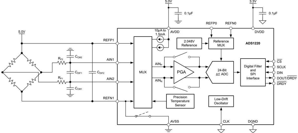
ADS1220 datasheet — Figure 9-11. Resistive Bridge Measurement, p. 62. Reproduced for reference.
Known limitation: The datasheet schematic values C_REF at 0.1 µF, but does not provide values for R_F1, R_F2, C_CM1, C_CM2, C_DIF1, or C_DIF2 in the bridge application schematic.
Supply Configuration
Figure 9-13 (page 64) outlines the unipolar supply connection for the 16-pin package. Although the datasheet description text labels it a "16-pin SOIC", the ADS1220 is offered only in 16-pin VQFN and TSSOP packages; the pinout shown matches these packages. Both AVDD and DVDD are driven at 3.3 V, decoupled to ground with 0.1 µF capacitors, with AVSS and DGND tied to ground.
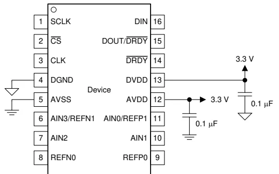
ADS1220 datasheet — Figure 9-13. Unipolar Analog Power Supply, p. 64. Reproduced for reference.
Figure 9-14 (page 64) provides the bipolar supply alternative. DVDD is supplied with 3.3 V (0.1 µF decoupling to DGND), while the analog core runs split rails: AVDD at 2.5 V (0.1 µF to ground) and AVSS at −2.5 V (0.1 µF to ground).
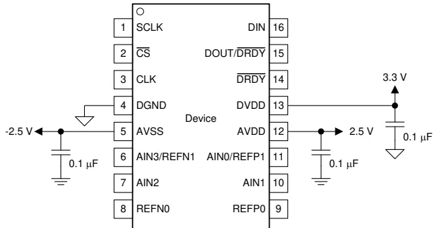
ADS1220 datasheet — Figure 9-14. Bipolar Analog Power Supply, p. 64. Reproduced for reference.
Known limitation: The datasheet illustrates unipolar operation at AVDD = 3.3 V (Figure 9-13), bipolar at AVDD = 2.5 V / AVSS = −2.5 V (Figure 9-14), and ratiometric bridge operation at AVDD = 5.0 V (Figure 9-11). These rail voltages reflect application requirements rather than a single fixed operating voltage.
Layout
Figure 9-15 (page 65) illustrates high-level partitioning between analog signal conditioning, the ADC device, the host microcontroller, and the transceiver interface, identifying the option for a split ground cut.
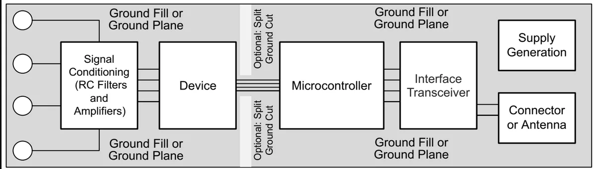
ADS1220 datasheet — Figure 9-15. System Component Placement, p. 65. Reproduced for reference.
Figure 9-16 (page 66) provides the device-level layout for the 16-pin package. Decoupling capacitors sit immediately adjacent to pin 12 (AVDD) and pin 13 (DVDD). Input filter components surround AIN0–AIN3 and REFP0/REFN0, with series resistors on the digital lines (DRDY, DOUT, DIN, SCLK, CS). Ground pins AVSS (pin 5) and DGND (pin 4), along with CLK (pin 3), tie directly to ground plane vias.
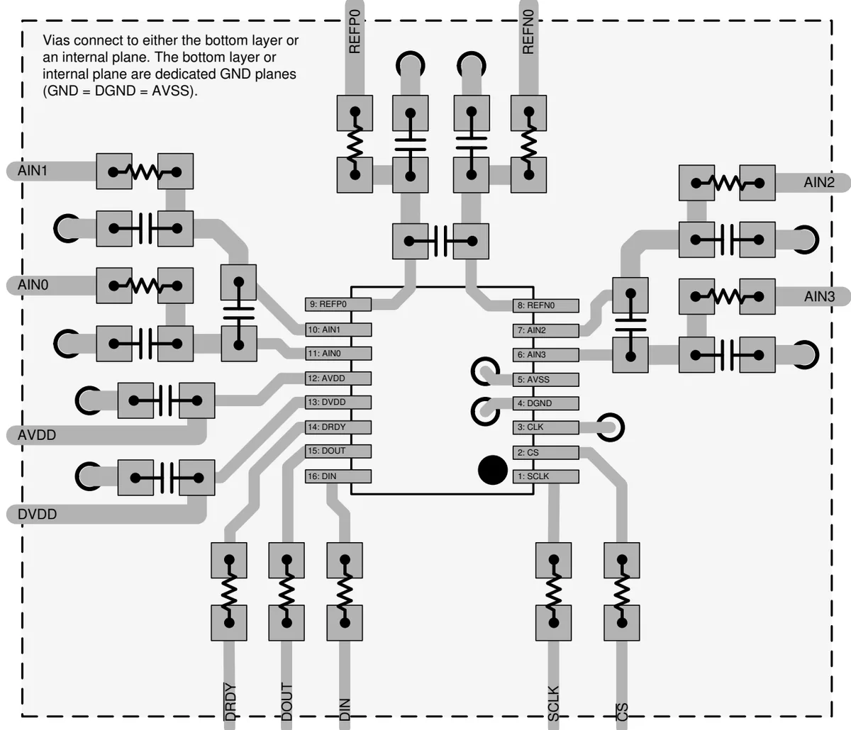
ADS1220 datasheet — Figure 9-16. Layout Example, p. 66. Reproduced for reference.
Known limitation: Figure 9-16 illustrates component footprints and routing topology for input filters and reference bypass networks, but omits specific component value callouts on the drawing itself.
Shared Pin Constraints
Figure 8-1 shows that AIN0 shares a physical pin with REFP1, and AIN3 shares a physical pin with REFN1. The resistive bridge in Figure 9-11 uses REFP1/REFN1 for excitation sensing, which leaves AIN1 and AIN2 as the available differential inputs. Conversely, the thermocouple (Figure 9-3) and RTD (Figure 9-6) topologies use the dedicated reference pair REFP0/REFN0, freeing AIN0 and AIN3 for input sensing and IDAC routing. Additionally, only the negative reference input on REFN1 connects to the internal low-side power switch.
Bring-Up Sequence
- Verify Supply Rails: Verify DVDD is 3.3 V with 0.1 µF decoupling to DGND. For unipolar designs (Figure 9-13), verify AVDD is 3.3 V (or 5.0 V per Figure 9-11) and AVSS is 0 V. For bipolar designs (Figure 9-14), confirm AVDD is 2.5 V and AVSS is −2.5 V.
- Clock Source: If using an external clock on pin 3 (CLK), verify frequency is within 500 kHz to 4.5 MHz (4.096 MHz nominal). If using the internal oscillator, confirm pin 3 is tied directly to DGND per Figure 9-1 and Figure 9-16.
- SPI Continuity: Verify continuity through the 47 Ohm series resistors on CS, SCLK, DIN, DOUT/DRDY, and DRDY.
- Reference Pair Selection: Confirm whether the firmware configures the reference multiplexer for REFP0/REFN0 (Figure 9-3, Figure 9-6) or REFP1/REFN1 (Figure 9-11). If using the low-side power switch, confirm REFN1 is the selected negative reference.
- Passive Network Verification: Confirm component placement against topology requirements: R_F1 = R_F2 = 1 kOhm, C_DIF = 100 nF, C_CM1 = C_CM2 = 10 nF for thermocouples (Figure 9-3); R_REF = 1.65 kOhm for 3-wire RTDs (Figure 9-6); C_REF = 0.1 µF across excitation rails for bridge circuits (Figure 9-11).
Troubleshooting
- No SPI Response: Inspect the 47 Ohm series resistors on SCLK, CS, DIN, and DOUT/DRDY for opens. Confirm pin 3 (CLK) is tied to DGND if relying on the internal oscillator. Verify DVDD is 3.3 V at pin 13 with its 0.1 µF capacitor intact.
- Conversion Value Scaled Incorrectly: Check the reference multiplexer register settings. If using the external reference inputs, verify voltage is present across REFP0/REFN0 or REFP1/REFN1 corresponding to the active register configuration.
- Thermocouple Measurement Offset: Verify external filter passives: R_F1 = R_F2 = 1 kOhm, C_DIF = 100 nF, C_CM1 = C_CM2 = 10 nF. Check that bias resistors R_B1 and R_B2 establish the common-mode voltage within PGA limits.
- RTD Reading Changes with Wire Length: Confirm R_REF is 1.65 kOhm. Verify the cutoff frequency of the reference filter (R_F3, R_F4, C_DIF2, C_CM3, C_CM4) matches the analog input filter (R_F1, R_F2, C_DIF1, C_CM1, C_CM2).
- Bridge Reading Drift or Inactivity: Verify AVDD is 5.0 V and C_DIF2 is installed across REFP1 and REFN1. If the low-side switch is enabled, verify continuity through pin 6 (AIN3/REFN1) to AVSS when closed (internal R_ON is 3.5 Ohm typ, 5.5 Ohm max).
- Analog Input Railing: Check if an input channel overlaps with an active reference line: pin 11 serves as both AIN0 and REFP1; pin 6 serves as both AIN3 and REFN1.
Parametric Reference
- Resolution: 24 bits typical; 4 single-ended or 2 differential channels.
- External clock frequency: 500 kHz min, 4.096 MHz typ, 4.5 MHz max.
- CMRR: at DC, Gain = 1: 90 dB min, 105 dB typ. At f_CM = 50 Hz or 60 Hz, DR = 2000 SPS: 95 dB min, 115 dB typ.
- Input offset voltage: Gain = 1, differential inputs, T_A = 25 °C: −30 µV min, 4 µV typ, 30 µV max. Gain = 2 to 128: 4 µV typ, 30 µV max. PGA disabled, Gain = 1 to 4: 4 µV typ, 30 µV max.
- Input offset voltage drift: Gain = 1 to 128, T_A = −40 °C to +85 °C: 80 nV/°C min, 300 nV/°C max. Over full temperature range: 250 nV/°C typ, 300 nV/°C max.
- PSRR: AVDD at DC, V_CM = 0.5 AVDD, Gain = 1: 80 dB min, 105 dB typ. DVDD at DC, Gain = 1: 100 dB min, 115 dB typ.
- Operating temperature range: −40 °C to +125 °C.
- Digital outputs: V_OH = 0.8 V min at I_OH = 3 mA; V_OL = 0.2 V max at I_OL = 3 mA.
- Power dissipation: 0.4 mW typ in duty-cycle mode (PGA disabled); 1.4 mW typ in normal mode (Gain = 1 to 16); 2.1 mW typ in turbo mode (Gain = 1 to 16).
- Propagation delay: DOUT load = 20 pF || 10 kOhm to DGND: 50 ns max.
- Sample rate: programmable up to 2000 SPS.
- Settling time: 0.05 s typ in normal mode at 20 SPS (single-cycle settling).
- Low-side power switch on-resistance: 3.5 Ohm typ, 5.5 Ohm max.
- Absolute maximum ratings: Supply voltage −0.3 V to 7.0 V; AVSS to DGND: −2.8 V to 0.3 V.
- Quiescent current in power-down mode: I_AVDD = 100 nA typ, 3 µA max; I_DVDD = 300 nA typ, 5 µA max. Normal mode (Gain = 1 to 16): I_AVDD = 340 µA typ, 490 µA max; I_DVDD = 75 µA typ, 110 µA max.